Binary Clock
Version two of my binary clock electronics project, using a Raspberry Pi. Written in C++ with a threaded web server for front-end configuration.
Purpose

The purpose of this project was to experiment with the Raspberry Pi, electronics and C++; I also wanted to create a new binary-clock with internet-updated time, the ability to set multiple alarms by using a web-browser (alarm clock), a multi-threaded custom-written web-server and room automation based on sensor data.
This was a continuation of an older, version one, binary clock (pictures at the very bottom of the page).
Gallery
-
 Shift registers for controlling multiple LEDs with three GPIO inputs
 -
 Binary clock with side open
 -
 Binary clock's homepage, served by the program its self. Written in C++ and multi-threaded using C++ 11.
 -
 Binary clock options
 -
 Guest book with IP geo-location using IP block lists from APNIC
 -
 Template and resource caching; assets are kept in memory to reduce I/O for high performance
 -
 Database test connection page
 -
 The services within the C++ program, which can be independently controlled and fail
 -
 Website tools menu
 -
 System information viewer
 -
 Website read-only API
 -
 Random number generator, using analogue data as seed
 -
 Binary clock GPIO menu, allowing conditions to turn actual power sockets on/off
 -
 An example GPIO configurer, which is linked to a power socket and turns it on/off based on the amount of light in the room
Using a Basic Shift Register
Hardware Communication
Due to the number of limited outputs on the Raspberry Pi, it’s practical to use a shift-register to virtually increase the number of outputs; for a basic 24-hour binary clock, you will require at least 17 LEDs - which would consume nearly all of the usable output ports on the Raspberry Pi.
The following section is about the 74HC595, an integrated-circuit with 16 pins; the 74HC595 is practical because eight pins can be utilized as output’s and multiple IC’s can be connected in series - it’s also very cheap. To control 17 LEDs to display binary time, we shall use three shift registers (allowing for up to 24 outputs)…which requires only three output pins from our Raspberry Pi.
Pin layout: 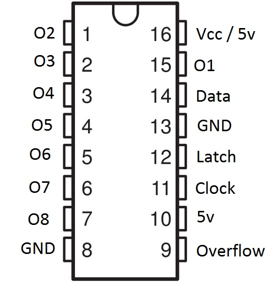
To control each of the eight output pins (O1-O8), we must communicate using three pins (which are connected to our Raspberry Pi):
- Latch - we set the latch to low when we want to write new data to our shift register; we then put it back to high when we’re finished.
- Data - specifies if an output pin is enabled.
- Clock - we toggle the clock, by setting it to high and then low, to get the shift register to read the value of the data-pin.
Therefore to set the eight outputs of a shift register to on/off, we would do the following:
- Set the latch to low.
- For each output pin in order from 1 to 8:
- Set the data-pin to high or low to specify if a pin is either enabled or disabled.
- Toggle the clock by setting it to high and then setting it back to low; this will cause the shift register to set the pin either on/off based on the data-pin.
- Set the latch back to high.
When we want to control more than eight pins, i.e. multiple shift-registers in-series, we simply repeat step 2 (setting which pins to be on/off) sixteen times. However each shift-register in-series is connected like a chain; every shift-register after the first has its data-pin connected to the previous shift-register’s overflow pin (refer to pin-layout). Therefore when the first eight pins have been set on the primary shift-register, the data signal is pushed to the overflow pin - which goes to the data-pin of the next/second shift-register; this continues until the latch is set back to high at the end.
The clock and latch is therefore connected to each shift-register using the same circuit, hence for our 17 LEDs we end-up with the following circuit (click to open the image):
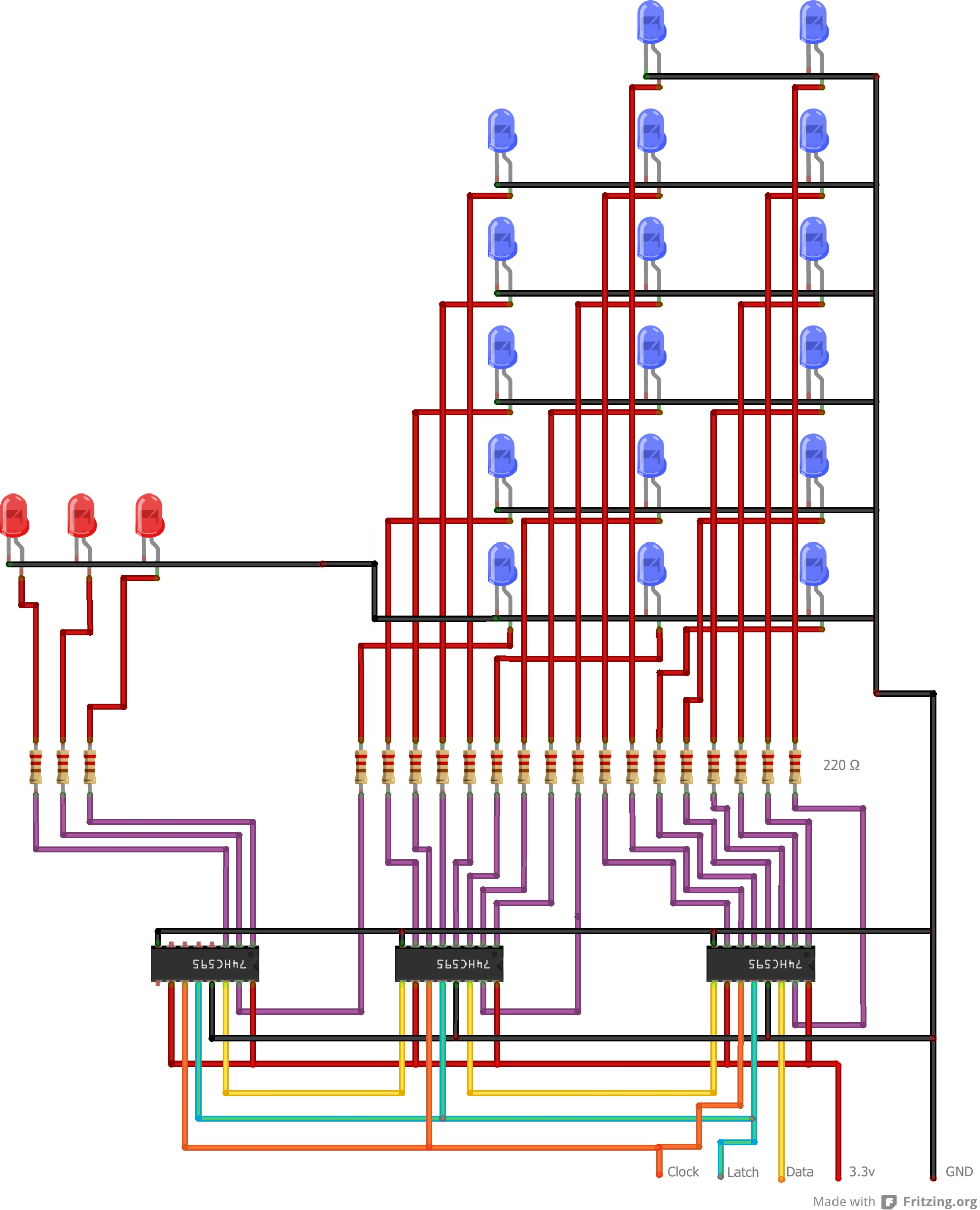
This diagram may look scary at first, however follow the circuit for the data-pin and re-read the above paragrah - you should see that the primary/first shift-register is the right-most shift-register.
Software Communication
In this video, a simple binary count is performed to test the circuit on a bread-board:
I do not have the actual code available for the above test, due to corruption with the Debian image; however the code used the shiftOut function of the WiringPi library, which worked something like this:
    uint8_t pinData = 0, pinLatch = 2, pinClock = 3;

    pinMode(pinData, OUTPUT);
    pinMode(pinLatch, OUTPUT);
    pinMode(pinClock, OUTPUT);

    while(true)
    {
      for(int i = 0; i < 8; i++)
      {
        digitalWrite(pinLatch, LOW);
        shiftOut(pinData, pinClock, MSBFIRST, i);
        digitalWrite(pinLatch, HIGH);
        usleep(1000 * 100); // 100 m/s delay
      }
    }
I then improved the code by creating a wrapper to allow for multiple shift-registers:
    uint8_t pinData = 0, pinLatch = 2, pinClock = 3;

    pinMode(pinData, OUTPUT);
    pinMode(pinLatch, OUTPUT);
    pinMode(pinClock, OUTPUT);

    while(true)
        for(int i = 1; i <= 32768; i*= 2)
        {
            IC_74HC595::write(2, pinData, pinLatch, pinClock, i);
            //std::cout << i << std::endl;
            usleep(1000 * 10); // 10 m/s delay
        }
The write member-function:
    inline static void write(uint8_t numberOfShiftRegisters, uint8_t pinData, uint8_t pinClock, uint8_t pinLatch, int value)
    {
        // Place latch to low, to write data
        digitalWrite(pinLatch, LOW);
        // Write the eight bits
        for(int i = (8 * numberOfShiftRegisters) - 1; i >= 0; --i)
        {
            // Set data-pin to on or off
            digitalWrite(pinData, value & (1 << i));
            //std::cout << "74HC: " << i << " - " << (value & (1 << i) ? 1 : 0) << "!" << std::endl;
            // Inform the IC to read the data-pin
            digitalWrite(pinClock, HIGH);
            digitalWrite(pinClock, LOW);
        }
        // Put the latch back to high
        digitalWrite(pinLatch, HIGH);
    }
Analogue Sensors
Since my new binary clock will be responsible for partial room-automation, I wanted to add sensors; using sensor data and specified thresholds, certain electrical appliances can be turned on/off etc.
Hardware Communication
Since I decided to use a photo-resistor and TMP36 temperature sensor, we require analogue inputs to read their values; however the Raspberry Pi does not have any analogue inputs (only digital / high and low). Therefore the solution is to use an analogue-to-digital converter, which translates an analogue signal (0 to 1023 - since the MCP3008 has a 10-bit resolution / 2^10-1=1023 ~ we subtract one since we start at zero of-course) to on/off (compatible with our Raspberry Pi); I have decided to use the MCP3008 because it’s fairly simple to use.
Pin layout:
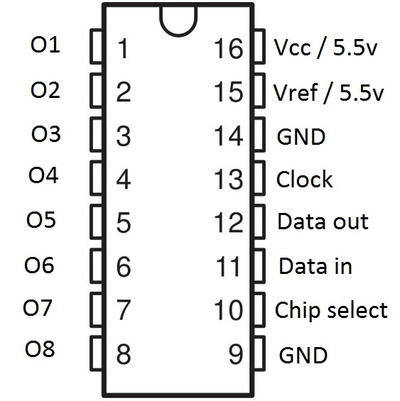
The MCP3008 requires four pins on the Raspberry Pi:
- Clock - used to specify when the data-in pin has been set; the same principal as the clock from the shift-registers previously mentioned; this will also be used to read bits out as well.
- Data-out - used for reading bits, or rather high’s and/or low’s, which represent the numeric value of a pin (from 0 to 1023 due to being analogue).
- Data-in - used to specify which pin’s value to output on the data-out pin.
- Chip-select - a similar function to the latch of a shift-register in this context, click here for more information.
Software Communication
According to the data-sheet, the following takes place to read a single-pin on the MCP3008 (which has eight analogue inputs):
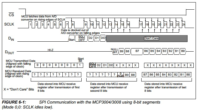
Transmitting the Pin to be Read
Therefore to read a pin we need to transmit the following on the data-in pin:
- Specify high (1) as our start-bit.
- Specify high (1) to state the input-mode as single-ended
- Three bits representing a number between 0 to 7, stating which pin to read; if you do not know binary:
- 000 = 0
- 001 = 1
- 010 = 2
- 011 = 3
- 100 = 4
- 101 = 5
- 110 = 6
- 111 = 7
Reading the Value of the Pin
After the above takes place, we then need to read data from the data-out pin:
- Read an empty-bit.
- Read a null-bit.
- Read ten bits representing the value (from 0-1023 / 2^10 - 10 bits) of the analogue pin.
During each read, we will toggle the clock (set it to high and then low) to inform the MCP3008 we have read the data-out pin.
Putting It Together
Hence to read the value of a pin on the MCP3008, using the previously mentioned procedures and communication diagram, we do the following:
- Inform the MCP3008 we want to read a pin, using a procedure equivalent to the latch with shift-registers:
- Set the chip-select pin to high.
- Set the clock pin to low.
- Set the chip-select pin to low.
- Write five-bits of data to inform the MCP3008 of the pin to be transmitted:
- Two bits set to high (our start-bit and to state the transmit mode as single-input).
- Three bits representing a value from 0-7, corresponding to the pin to be read.
- Read 12-bits of data:
- An empty-bit.
- A null-bit.
- Ten bits representing the value of the pin from 0 to 1023.
- Inform the MCP3008 we have finished this cycle; again, equivalent to a latch with shift-registers:
- Set the chip-select to high.
This is the following function I wrote, with help from a Pastebin entry by Dvanhaeke for transmitting the five-bits:
    int IC_MCP3008::read(MCP3008_PINS pin, uint8_t pinDataIn, uint8_t pinDataOut, uint8_t pinClock, uint8_t pinChipSelect)
    {
        if(pin < 0 || pin > 7)
            return -1;
        // With help from: http://pastebin.com/62rXCzej
        // Toggle chip-select for the MCP3008 to accept clock low-state
        digitalWrite(pinChipSelect, HIGH);
        digitalWrite(pinClock, LOW);
        digitalWrite(pinChipSelect, LOW);

        // Write 5-bits of data to the MCP3008
        // Structure:
        //          < 11 to state start-bit and single-ended input mode >
        //          < three bits 0-7 to state the pin being read >
        // Source: http://ww1.microchip.com/downloads/en/DeviceDoc/21295d.pdf, page 19
        int value = pin;        // Pin (0-7) being read
        value |= 0x18;          // pin + 11000 (24 / 0x18)
        value <<= 3;            // Shift three places 11< pin >000
        for(int i = 0; i < 5; i++)
        {
            // 10000000 (0x80 / 128)
            digitalWrite(pinDataIn, value & 0x80 ? HIGH : LOW);
            value <<= 1;
            // Toggle clock to cause the MCP3008 to read the value of the data-in pin
            digitalWrite(pinClock, HIGH);
            digitalWrite(pinClock, LOW);
        }

        // Read 12-bits form the MCP3008 (null bit, empty bit and 10 bits representing the value of the pin being read)
        value = 0;
        for(int i = 0; i < 12; i++)
        {
            // Toggle clock to cause the MCP3008 to write the next bit of data to data-out pin
            digitalWrite(pinClock, HIGH);
            digitalWrite(pinClock, LOW);
            // Shift the current value by one, ready for the next bit of data to be read
            value <<= 1;
            // Read the next bit of data
            if(digitalRead(pinDataOut) == HIGH)
                value |= 0x1;
        }
        // Toggle chip-select pin, end of read
        digitalWrite(pinChipSelect, HIGH);
        // Get rid of the first bit (null)
        value /= 2;
    }
If you’re still unsure, I would also recommend reading the article by Jeremy Blythe from his article on the MCP3008.
Hardware Sensors
I am using the MCP3008 to read the temperature and the amount of light using a photo-resistor; the circuit looks like the following:
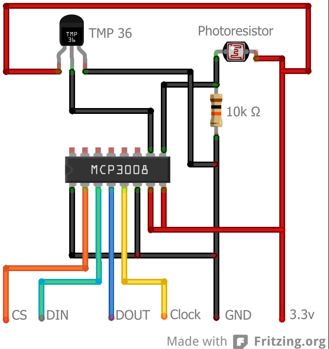
Photo-Resistor - Light Sensor
The photo-resistor simply requires 3.3v to one pin, it doesn’t matter which end; then you need to wire the other pin to an analogue-input and have the same wire also connected to a 10k resistor, which is then connected to ground. The way the photo-resistor works is by specifying a value between 0 to 1023 (for a 10-bit analogue-to-digital converter) based on dark to light; hence in a pitch-black room, the photo-resistor should read 0 - therefore in a very bright room, it should read 1023. We can then convert this to a percentage using very basic maths:
\begin{align} (input value / 1023) * 100 \end{align}
TMP36 - Temperature Sensor
The wiring of pins on the TMP36 [b]does matter[/b]; with the flat-side of the TMP36 facing you, the pins should be wired in the following order:
- 3.3v input
- Analogue input
- Ground (no resistor required)
The TMP36 will also output a value between 0 to 1023 (for a 10-bit analogue-to-digital converter); we convert it to celcius using the following formula:
\begin{align} (voltage~in~millivolts - 500) / 10 = celcius \end{align}
To convert our 3.3v analogue signal to millivolts, we use the following formula:
\begin{align} analogue * (3.3 * 1000) / 1024 = analogue~in~millivolts \end{align}
Hence we end up with the following formula to convert the raw analogue signal to a temperature in celcius:
\begin{align} ((analogue * ((3.3 * 1000) / 1024)) - 500) / 10 = celcius \end{align}
The code I wrote to read the TMP36:
    inline static double getTemperature_Celcius(double volts, IC_MCP3008::MCP3008_PINS pin, uint8_t pinDataIn, uint8_t pinDataOut, uint8_t pinClock, uint8_t pinChipSelect)
    {
            return ((getRaw(pin, pinDataIn, pinDataOut, pinClock, pinChipSelect) * ((volts * 1000) / 1024)) - 500) / 10; // ([voltage in millivolts] - 500) / 10; volts to millivolts = [value] * ([[volts e.g. 3.3 or 5]v * 1000] / 1024)
    }
Tips
Debugging with Root
I did try the following with the WirePi library:
    sudo chown root binaryclockv2
    sudo chmod 4755 binaryclockv2
Even though no errors were thrown and the setup was successful, I could not set a GPIO to high; additionally this had to be set after every build. Instead I simply did:
sudo passwd root
…and then I connected, via remote development, using the root account. The above command sets the password for the root account, which by default is not set on Debian squeeze (the distribution used on my Raspberry Pi).
This is bad security practice, however the Raspberry Pi was on a secure network and the context was strictly for debugging. You can alternatively, apparently, install the WirePi library as programs, which can be executed without sudo/super-user privileges, however I decided against this due to decreased speed.
Constructing & Debugging Physical Circuit Boards
I would recommend purchasing a digital multimeter and testing your circuits; for this binary clock, I used sockets (which are used to hold integrated circuits such as the 74HC595 shift-register). I would then leave the sockets empty and use my multimeter to test the voltage through each pin to check no pins were touching. Using a socket will also prevent heat-damage to the IC from a soldering iron.
Useful Links
Below are a collection of links I found to be useful during this project; some of these links may contain articles written more towards your learning-style or contain more technical information.
- WiringPi library, a wrapper for the GPIO pins:
https://projects.drogon.net/raspberry-pi/wiringpi - Useful information regarding the GPIO pins:
http://elinux.org/RPi_Low-level_peripherals - Interfacing with the MCP3008 (analogue to digital converter) using a Raspberry Pi:
http://jeremyblythe.blogspot.co.uk/2012/09/raspberry-pi-hardware-spi-analog-inputs.html - A freeware application used for the circuit-drawings in this article:
http://fritzing.org
Source-Code
The source-code for this project can be found at Github:
https://github.com/limpygnome/binary_clock_v2
History
The binary clock presented in this article is version two, with the original version created using a Netduino. Below are some historic pictures, before the final binary clock.
 A picture showing the internal relays used to control actual power sockets, with v2 unpainted
  The front of version one, built using a Netduino
  The back of version one, with far more primitive circuitry
Comments